


In the field of LED display packaging, the core difference between GOB and COB stems from the fundamental positioning of their packaging systems:
GOB is a protective upgrade solution for traditional SMD packaging, retaining independent SMD LED chips throughout the process;
COB, on the other hand, is a completely new chip-level packaging system that bypasses the pre-fabrication of LED chips, resulting in no independent LED chip structure.
The technical characteristics, performance, and application suitability of both are centered around this core difference, and all descriptions are based on actual industry technical specifications and application status.
Essential Differences in Packaging Principles and Process Routes
COB (Chip On Board)
COB is a new packaging mode starting from the chip end. The core principle is that it does not require prefabricated SMD LED chips; instead, the LED chips are directly fixed to the PCB substrate, and electrical connections are achieved through wire bonding.
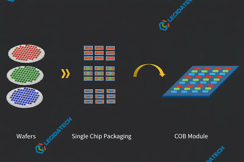
The process is completed through phosphor coating, overall encapsulation protection, and dicing.
In this entire process, the chip and the PCB substrate are directly interconnected, without an independent LED chip stage, making it a typical “chip-level” packaging process.
GOB (Glue On Board)
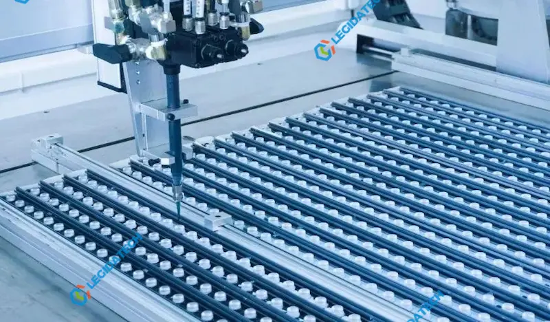
GOB is essentially a supplementary upgrade to SMD packaging. The process is built on the mature SMD packaging foundation: first, SMD LED chips are purchased and reflow soldered.
After module testing and surface cleaning, a highly transparent special protective adhesive is applied to the module surface. After curing, the finished product is tested.
This process does not change the core electrical structure of SMD packaging; it only adds an integrated protective layer to the LED chips and solder joints through the gluing process, retaining the essential characteristics of SMD point light sources.
Core Differences in Key Performance
Pixel Density and Resolution:
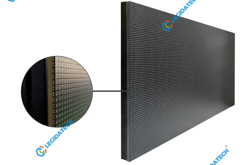
Due to the elimination of the physical limitations of LED chip brackets, COB has a higher pixel density limit and is mainly used in ultra-small pitch indoor applications from P0.4 to P1.2, making it a core technology for achieving ultra-high-resolution displays.
GOB is limited by the size of SMD LED chips, resulting in a lower resolution limit, mainly suitable for medium- to high-pitch applications from P1.0 to P2.5, and it is difficult to break through the P0.8 pitch limit.
Protection Capability:
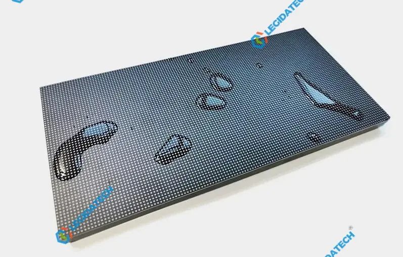
Both offer better protection levels than traditional bare-board SMD, reaching IP54 to IP65 levels, but the protection logic is different.
COB utilizes a fully sealed integrated packaging, completely isolating the chip from the external environment, providing superior moisture and dust protection.
GOB achieves protection through a surface adhesive layer, primarily protecting the surface and solder joints of the LED beads. The protective effect is concentrated on the module surface, and the sealing performance is slightly inferior to COB.
Heat Dissipation Performance:
In COB, the chip is in direct contact with the PCB substrate, allowing for direct heat conduction, resulting in lower thermal resistance and better heat dissipation efficiency.
This effectively improves the long-term operational stability of the display screen and is suitable for 7×24 continuous operation scenarios; the adhesive layer in GOB forms a slight thermal insulation layer, which does not affect normal use but slightly reduces heat dissipation efficiency.
High-power applications require additional reinforced heat dissipation design.
Display Effect:
COB has no lamp brackets, creating a smooth, continuous light surface. This removes dark gaps and “grainy” effects between LEDs, delivering better brightness uniformity, higher contrast, less glare, and more delicate visuals.
GOB uses a protective glue layer that improves optical refraction and reduces the point-light effect of SMD LEDs. However, because it still uses separate LED beads, the overall display uniformity and image smoothness are slightly lower than COB.
Maintenance and Cost:
In terms of maintenance, COB uses chip-level integrated packaging. Faulty units require factory repair with professional equipment, resulting in longer repair cycles and higher costs.
GOB retains the electrical connection structure of SMD LED beads, allowing for on-site replacement of individual faulty beads by peeling off the local adhesive layer.
This results in lower maintenance difficulty and controllable after-sales costs. In terms of cost structure, COB does not require the purchase of SMD LED beads, resulting in lower material costs, but the die bonding and wire bonding processes require high precision, and yield significantly impacts costs.
GOB requires additional investment in SMD LED beads and potting materials, resulting in higher material costs, but it is compatible with existing SMD production lines, has lower process difficulty, and has a stable yield, making it more cost-effective for medium- to high-pitch applications.
Summary of Core Advantages and Disadvantages
COB LED Packaging
Advantages
Focus on display performance and long-term stability: strong resolution breakthrough capability, suitable for ultra-small pitch high-end requirements;

excellent heat dissipation efficiency, extending service life; excellent display uniformity and visual experience, without graininess and glare; A fully sealed structure provides more thorough protection.
Disadvantages
stem from chip-level packaging characteristics: difficult to repair, insufficient on-site maintenance capabilities.
High production process threshold requiring strict equipment and technical standards and slightly lower brightness at the same power consumption, requiring optical compensation in high-brightness scenarios.
GOB Packaging
Advantages:
The protective glue layer greatly reduces the chance of LED lamp bead drop-offs and improves impact and collision resistance. Works well in harsh environments and mobile display setups.
Fully compatible with existing SMD production lines, keeping costs and technical barriers low. Supports on-site partial repair, making maintenance easier and more cost-effective.
Offers a great balance between protection and display performance, providing high cost-effectiveness in mid- to high-end applications.
Disadvantages:
GOB still depends on the SMD packaging structure, and the glue layer can affect heat dissipation, requiring better design for high-power displays.
The resolution limit makes it hard to achieve ultra-fine pixel pitch levels. The glue layer can cause 10–15% brightness loss, which needs to be compensated through LED selection or driver circuit design.
Learn More:
Understanding the Differences Between SMD and COB in LED Display Technology
DIP, SMD, and COB LED displays: The ultimate guide
Application Scenario Adaptation Principles
COB is primarily suitable for indoor ultra-small pixel pitch high-end display scenarios, such as command and control centers, high-end conference rooms, and broadcast television studios.
These scenarios have extremely high requirements for resolution, display uniformity, and long-term operational stability and are less sensitive to maintenance cycles.
GOB is more suitable for outdoor/semi-outdoor display scenarios and rental/mobile display scenarios, such as outdoor advertising screens, sports stadium displays, and stage rental screens.

These scenarios prioritize protection capabilities, impact resistance, and convenient on-site maintenance, with a focus on medium to high pixel pitch.
In conventional commercial indoor display scenarios around P1.0, both can be flexibly chosen based on project budget, display effect requirements, and maintenance needs.
Summary and Industry Development Trends
GOB and COB are not substitutes for each other but rather technical differentiations addressing different needs:
COB is a chip-level packaging revolution for ultra-high-definition displays, primarily addressing the limits of resolution and display performance.
GOB is an upgrade of SMD packaging for practical applications, primarily addressing the pain points of protection and maintenance.
The industry trend shows that COB technology is moving toward flip-chip design, phosphor-free quantum dot coating, and integrated driver ICs. The main goals are to simplify production, improve yield rate and cost performance, and strengthen COB’s lead in the ultra-fine pitch display market.
GOB technology is focusing on glue material optimization—improving transparency and reducing thermal resistance to minimize optical and heat loss. With improved lamination processes, GOB aims to expand its use in outdoor small-pitch LED displays.
Both technologies will jointly squeeze the market share of traditional bare-board SMD packaging, forming a differentiated competitive landscape in the ultra-high-end and mid-to-high-end markets.
Pingback: atorvastatin
Pingback: tadalafil cost